Rtl Code For Full Adder - Analysis And Implementation Of A Full Adder Circuit Using Xilinx / The full adder is a digital component that performs three numbers an implemented using the logic gates.
Get link
Facebook
X
Pinterest
Email
Other Apps
Rtl Code For Full Adder - Analysis And Implementation Of A Full Adder Circuit Using Xilinx / The full adder is a digital component that performs three numbers an implemented using the logic gates.. A synchronous digital circuit is modeled with following considerations: Cout is high, when two or more inputs are high. Design and implement a 4 bit full adder. Timescale directive is used for specifying the unit of time used in further modules and the time resolution (here one picosecond). The above code is written for half adder you may see no hierarchical style coding in it as half adder cannot be further divided but we can construct full adder by using two half adder which is shown below as well.
Yes, obviously sum is supposed to be connected to the module which requires the sum of a and b. The third bit is the carry bit. Here is a brief idea about binary adders. When i synthesize using xst and view the rtl schematic, i see the fas4.v module correctly with all the inputs. Once you understand how a full adder works, you can see how more complicated circuits can be built using only simple gates.
1 from Verilog hdl program for serial parallel. In this post, we will take a look at implementing the vhdl code for full adder using structural architecture. The signed full adder vhdl code presented above is pure vhdl rtl code so you can use it independently on every kind of fpga or asic. In_x = 0, in_y = 0, carry_in = 0, out_sum_fa = 0, out_carry_fa = 0 Design and implement a 4 bit full adder. Once the functionality of the circuit is verified. The following individual components have been modeled and have been provided with their corresponding test benches: But first lets see its simulated waveform:
Parrallel input serial output shift register (piso) (piso.v) d flip flop (d_flipflop.v) full adder (full_adder.v)
The sum s and the carry out c_out, where s=a^b^c_in, and c_out=ab+bc+ac, where ^ the xor logic operation and + is the logic or operation. Sum (s) output is high when odd number of inputs are high. When i synthesize using xst and view the rtl schematic, i see the fas4.v module correctly with all the inputs. 4optimized implementation of logic functions 4.12 cad tools 4.12.1 logic synthesis and optimization 4.12.2 physical design 4.12.3 timing simulation 4.12.4 summary of design flow 4.12.5 examples of circuits synthesized from verilog code A synchronous digital circuit is modeled with following considerations: Here given fig.1 is one bit half adder in the lowest level of the abstration diagram is there as similarly we know their are two ways to designed one bit full adder either using two half adder and one or gate or designed using their separate boolean expression as shown in below fig.2 and fig.3. Vhdl code of half adder using the dataflow model.it contains vhdl code for rtl diagram, simulation code and the waveform half adder. Parrallel input serial output shift register (piso) (piso.v) d flip flop (d_flipflop.v) full adder (full_adder.v) During the execution of code, i have used xilinx vivado software. Rtl schematic for full adder circuit testbench for full adder in verilog. This page of verilog sourcecode covers hdl code for half adder, half substractor, full substractor using verilog. The signed full adder vhdl code presented above is pure vhdl rtl code so you can use it independently on every kind of fpga or asic. The verilog codes are then simulated using the cadence nc sim and the waveform obtained on the graphical user interface is used to verify the operation of the adder incorporating the aforementioned optimization technique.
Mainly there are two types of adder: First, vhdl code for half adder was written and block was generated. In this post, we will take a look at implementing the vhdl code for full adder using structural architecture. If a carry generates on the addition of the first two bits, the full adder considers it too. Once you understand how a full adder works, you can see how more complicated circuits can be built using only simple gates.
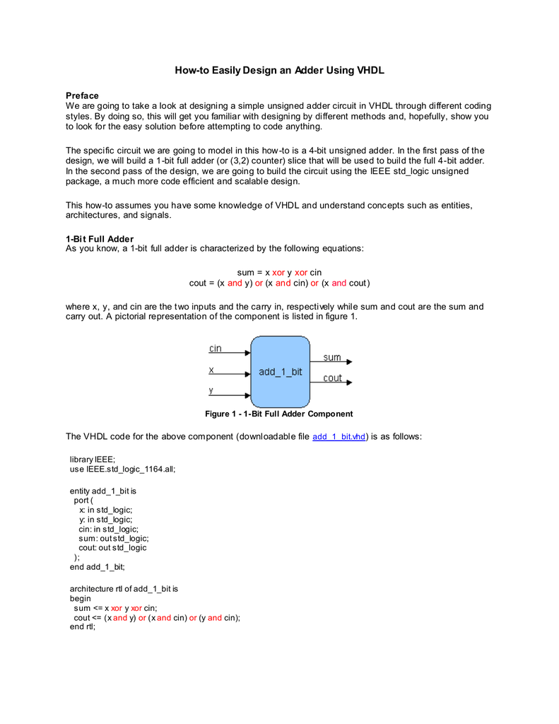
How To Easily Design An Adder Using Vhdl from s2.studylib.net In this post, we will take a look at implementing the vhdl code for full adder using the behavioral method. Here is a brief idea about binary adders. 4optimized implementation of logic functions 4.12 cad tools 4.12.1 logic synthesis and optimization 4.12.2 physical design 4.12.3 timing simulation 4.12.4 summary of design flow 4.12.5 examples of circuits synthesized from verilog code Full adder trial layout in figure1 is reported a trial layout on altera quartus ii using a cyclone v fpga. We'll first add the timescale directive. Redo the full adder with gate level modeling. Full adder module in vhdl and verilog. Integrated full adder has been designed,fig (2) shows vhdl code compilation of full adder with zero errors and zero warnings.fig(3)shows output waveform of full adder which verifies the truth table.fig (4)shows technological map view.fig(5)shows layout of full adder.fig(6) shows schematic of full adder in analog domain.
It is the main component inside an alu of a processor and is used to increment addresses, table indices, buffer pointers, and other places where addition is required.
A full adder, unlike the half adder, has a carry input. When i synthesize using xst and view the rtl schematic, i see the fas4.v module correctly with all the inputs. Design and implement a 4 bit full adder. Accordingly, the full adder has three inputs and two outputs. In_x = 0, in_y = 0, carry_in = 0, out_sum_fa = 0, out_carry_fa = 0 Half adder hdl verilog code. The third bit is the carry bit. As is customary in our vhdl course, first, we will take a look at the logic circuit of the full adder.since we are using the structural method, we need to understand all the elements of the hardware. Cout is high, when two or more inputs are high. Full adder module in vhdl and verilog. This repository contains behavioral code for serial adder. In this video we teach how to code for full adder in verilogmusic: Once the functionality of the circuit is verified.
Draw a truth table for full adder and implement the full adder using udp. Verilog hdl program for serial parallel. We'll first add the timescale directive. 4optimized implementation of logic functions 4.12 cad tools 4.12.1 logic synthesis and optimization 4.12.2 physical design 4.12.3 timing simulation 4.12.4 summary of design flow 4.12.5 examples of circuits synthesized from verilog code Accordingly, the full adder has three inputs and two outputs.
Synthesizing Full Adder With Ise Stack Overflow from i.stack.imgur.com Accordingly, the full adder has three inputs and two outputs. During the execution of code, i have used xilinx vivado software. The above code is written for half adder you may see no hierarchical style coding in it as half adder cannot be further divided but we can construct full adder by using two half adder which is shown below as well. Mainly there are two types of adder: It starts with a grave accent ` and does not end with a semicolon. This page of verilog sourcecode covers hdl code for half adder, half substractor, full substractor using verilog. Once the functionality of the circuit is verified. Cout is high, when two or more inputs are high.
Once you understand how a full adder works, you can see how more complicated circuits can be built using only simple gates.
Draw a truth table for full adder and implement the full adder using udp. A synchronous digital circuit is modeled with following considerations: Cout is high, when two or more inputs are high. The rtl codes are developed for full adder using both the designs. First, vhdl code for half adder was written and block was generated. It starts with a grave accent ` and does not end with a semicolon. Parrallel input serial output shift register (piso) (piso.v) d flip flop (d_flipflop.v) full adder (full_adder.v) Timescale directive is used for specifying the unit of time used in further modules and the time resolution (here one picosecond). I am trying to implement an 8 bit ripple adder using verilog on ise 11.5. It is the main component inside an alu of a processor and is used to increment addresses, table indices, buffer pointers, and other places where addition is required. Sum (s) output is high when odd number of inputs are high. And thus, since it performs the full addition, it is known as a full adder. Verilog and system verilog are programming languages designed to code hardware at register transfer level.
The full adder is a digital component that performs three numbers an implemented using the logic gates rtl code. // fpga4student.com // fpga projects, vhdl projects, verilog projects // verilog code for full adder // structural code for full adder module full_adder_structural_verilog( input x1, x2, cin, output s, cout );

Comments
Post a Comment